Industrial power applications generally require high input voltages. Standard voltages are 24V, 36V, and 48V. DC/DC step-down (buck) switching regulator controllers used in industrial application power circuits need to meet stable and reliable performance requirements in noisy, surge, and power outage environments.
Industrial system power requirements are often quite complex, often requiring voltage isolation to meet safety standards and suppress ground loop interference in noise-sensitive applications.
For example, in new factory automation systems such as PLCs and I/O modules, the number of I/O channels is increasing to improve sensing accuracy. Therefore, isolation between different voltages is the first choice for digital/analog signal isolation or channel-to-channel isolation to prevent common ground noise interference.
The traditional method of implementing this type of isolated power supply is to use a flyback power converter to generate the various voltages required for the bias supply. The flyback design generally uses an asymmetrical turns ratio of the primary and secondary coils of the transformer, as well as an optocoupler and a reference or auxiliary winding for feedback regulation. In addition, the flyback converter requires a carefully designed compensation circuit to ensure stability, which results in a cumbersome design process, a large number of components, and a large solution size and high cost.
This article introduces a simpler method to achieve isolated voltage without using a flyback topology.
Isolated Synchronous Buck Converter
The isolated buck converter uses a synchronous buck converter with a coupled inductor to generate an isolated output (see Figure 1). Since the transformer primary and secondary turns ratios are more closely matched, the isolated converter using this topology can achieve equivalent energy transfer using a smaller transformer. Because the secondary output closely matches the primary regulated output voltage, no optocoupler or auxiliary winding is required, which helps to reduce solution size and cost.
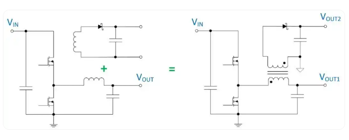
Figure 1. Isolated buck converter generating two outputs
This topology offers the following benefits:
Easy to generate positive and negative isolated supplies
Primary-side supply can power the load without being isolated from VIN
Simpler design compared to traditional flyback approach
Fewer solution components and smaller size than traditional flyback topology
To demonstrate the ease of designing this power supply, we use the SiC462, a member of the 6A family of fully integrated synchronous buck regulators. These devices offer high power conversion efficiency and power density with reduced parasitics due to excellent silicon (MOSFET and driver) and package design techniques.
The power stages used in this family can deliver 3A to 10A continuous current, depending on the model. The output voltage is adjustable from 0.8V to 0.9*VIN, with an input range of 4.5V to 60V. These devices have rich features such as multiple power saving modes with very low output operating current, adjustable operating frequency, fast transient response, cycle-by-cycle current limit, adjustable current limit, overvoltage protection (OVP), overtemperature protection (OTP), undervoltage protection (UVP), power good signal, tracking, sequencing, minimum operating frequency of 25kHz, ultrasonic mode to avoid audible noise, soft start, etc., and all-ceramic capacitor solutions are used for input and output. This flexibility allows us to design a power supply that generates two outputs, single isolation, with well-regulated output.
The basic requirements of this design are as follows:
VIN: 32V to 56V
VOUT: 12V at 2A, isolated 5V at 1A (called isolated +5)
Minimum load: 10% of full load value
The design is based on a dual-winding inductor buck regulator. The inductor "flyback" circuit is used to generate another output. This is a continuous flyback design, and the SiC462 always operates in full synchronous mode, even under no-load conditions. This is because the regulator has a “mode” select function. This function allows operation in different modes, depending on the specific requirements. There are two operating modes: “power save” mode, in which the regulator enters deep discontinuous operation and energy is only transferred to the output a few times per second, and “continuous mode” where energy is transferred during every switching cycle. Continuous operation at light loads is not very efficient; however, this mode of operation improves transient response and allows the addition of a flyback winding at light or zero load conditions.
In Figure 3, the inductor L1 consists of a high temperature powder toroidal core with 24 and 16 turns of bifilar windings for the “primary” and “secondary” respectively. This inductor was designed specifically for this project (not standard) and was built in our lab. Since the regulator main loop controls the voltage VOUT, the voltage across the inductor is kept constant when the low-side switch is on, as shown in Figure 2A.
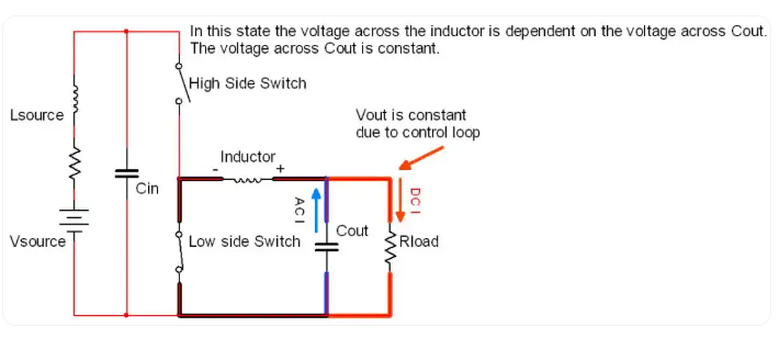
Figure 2A. Conventional buck converter operation with MOSFET on.
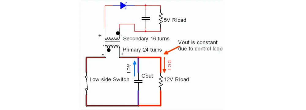 Figure 2B. "Flyback Transformer" Replaces Inductor
As shown in Figure 2B, when the low-side switch is on, the circuit becomes a simple half-regulated flyback circuit. The primary winding is 24 turns, and the voltage is 12V / 24 turns = 0.5V / turn.
Based on the flyback winding, 16 turns x 0.5V / turn = 8V. Considering the 0.65V drop across diode D1 in Figure 3, we get a result of 7.35V. In addition, the winding DCR and the flyback transformer coupling factor also produce voltage drops. Therefore, the result is about 6.5V. Note that the "blue dot" next to L1 represents the phase of the winding in Figure 2B and Figure 3. Now, we use "flyback transformer" interchangeably with "inductor".
As can be seen from the performance characteristics below (see Figures 6A and 6B), the input capacitor stress is greatly increased in this design. Due to the leakage inductance, a snubber circuit consisting of C27 and R17 is required across the diode D1 used at the flyback output. A snubber circuit consisting of C17 and R8 is required from the LX node to the power ground to limit the voltage peaks generated by the device parasitic effects on the SiC462.
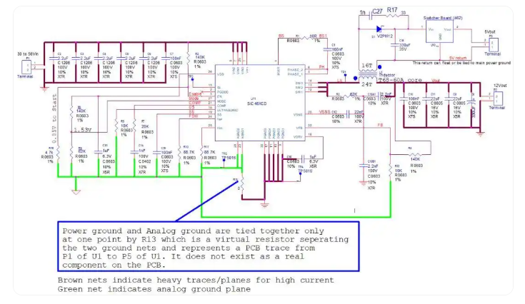
Figure 3. Dual output regulator circuit diagram
The flyback winding contributes to the circuit operation by keeping the inductance below the nominal value. Below are the various waveforms displayed on the oscilloscope (see Figure 3 for the circuit net and Figure 5 for the waveform description).
CH1, yellow: inductor current; inductor to Lx node current
Ch2, blue: Lx node voltage to ground
Ch4, green: flyback winding voltage between 5V return and D1 anode (across L116 turns)
Below are some example waveforms showing the circuit operation.
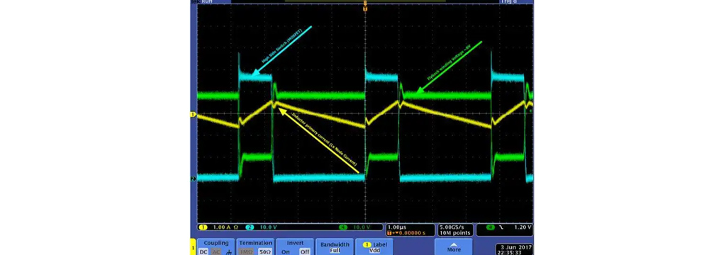
Figure 4. Waveforms at 45VIN with isolated +5 no load and main +12 0.2A
Figure 4 shows the “normal” buck waveforms in continuous current mode. The average current is 0.2A.
Now, we increase the +12 output (main winding) current to make the +5 isolated load current zero:
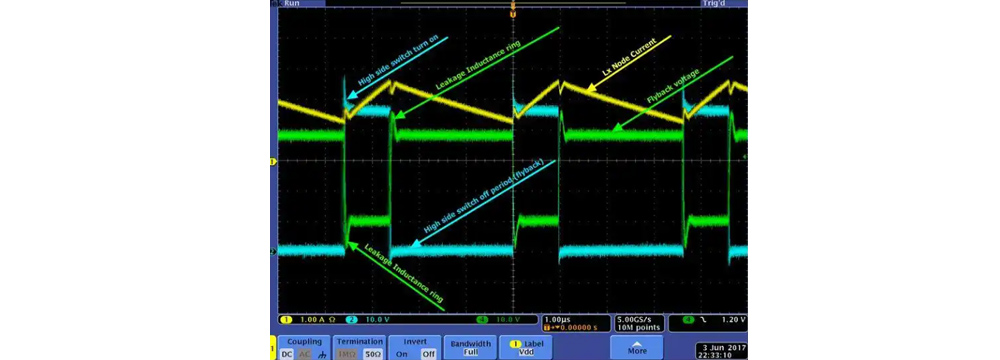
Figure 5. Waveforms at 45VIN with isolated +5 no load and main +12 2A
In Figure 5 above, the peak-to-peak current of the L1 main winding remains unchanged, but the average current increases.
Now, we increase the flyback winding current by adding a +5 isolated load and reducing the main winding current to zero:
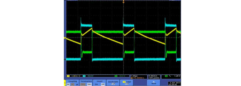
Figure 6. Waveforms at 45VIN when isolated +5 is fully loaded (1A) and main +12 is 0.2A
As shown in Figures 4 to 6, the flyback voltage (voltage across C16) remains basically unchanged under various operating conditions.
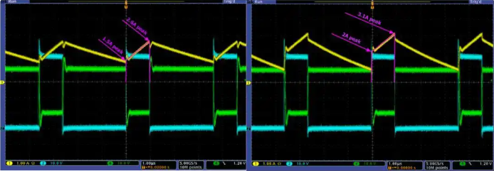
In Figures 6A and 6B, we show the high-side switch peak current as the magenta line, which is the same as the input capacitor ripple current. Note that the current peak increases significantly at the same operating point in both figures when loaded with 5V. This increased ripple current must be considered when selecting the input capacitor for this application and for any electromagnetic compatibility (EMC) requirements.
As shown in Figure 7, the efficiency curve is very flat over the input voltage range.
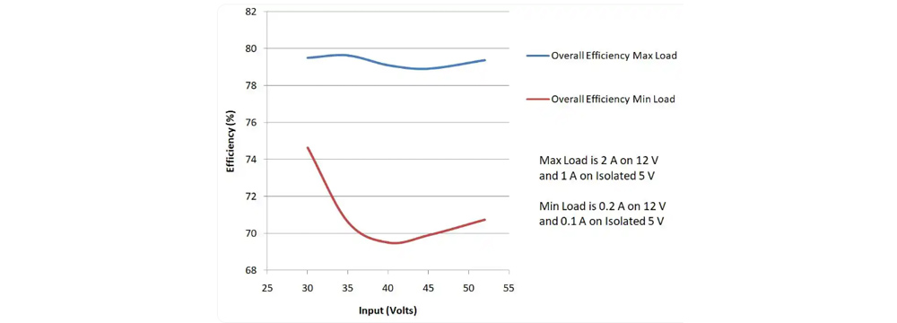
Figure 7. Efficiency curves over input voltage and load range (including secondary switching regulator, U10)
As shown in Figure 8, the main +12V output has excellent line regulation over a wide range of load conditions.
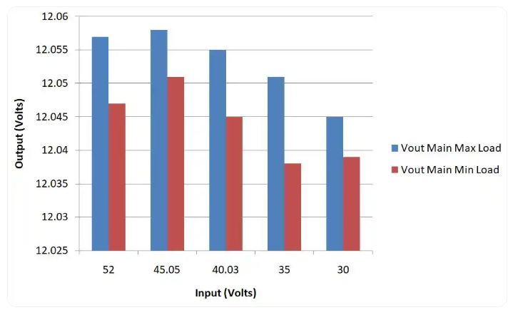
Figure 8. Main +12V Output Voltage Regulation for Various Output Loads and Line Voltage Conditions
The DC output voltage across the flyback winding C18 is not well regulated. About 10% linear regulation is achieved over a 32V to 56V input range. However, if the input bus VIN range is not as wide as in this design example, 3% to 4% linear regulation is reasonable for application purposes. If the linear regulation requirement is tighter or better performance is needed over a wider input voltage range, a switching regulator (U10 in Figure 2) or a linear regulator can be used.
Conclusion
PLC and I/O module power supply design becomes complex with the need for multiple isolated voltages, floating bias voltages, and negative output voltages. PLCs are widely used in factory automation, building automation, and process control. The requirements for different isolated power supplies for gate drivers, operational amplifiers, and isolated communication interfaces such as RS-485, RS-232, etc., require simpler methods to generate these voltages while meeting the requirements of reduced component count, smaller PCB size, and low-profile compact designs.
This analog board design is an example of the new designs enabled by the introduction of high-voltage series buck regulators such as the SiC462.
Share our interesting knowledge and stories on social media


