1. The basic principle of isolated power supply
Isolated power supply is an electrical device that cuts off the direct electrical connection between input and output circuits by physical isolation. Its core functions include safety isolation, elimination of ground interference and protection of circuit integrity. The device uses transformers, optocouplers and other components to achieve electrical isolation, and has protection functions such as overvoltage and short circuit. It is widely used in medical equipment, industrial control systems and other scenarios with high safety requirements. Compared with non-isolated power supplies, it is safer but more expensive, and the use scheme needs to be selected according to specific needs
2. The role of high-voltage capacitors
2.1 Filtering and ripple removal: High-voltage capacitors are used in power supply and signal processing circuits to filter and remove ripples in power supplies. By absorbing and smoothing the pulsating voltage in the power supply, stable power supply in the circuit is ensured.
2.2 Energy storage and release: High-voltage capacitors can store a large amount of charge and release energy quickly when needed. This makes them very important in pulse power applications, energy recovery systems and high-frequency circuits.
2.3 Voltage compensation: In the power system, high-voltage capacitors are used for voltage compensation and reactive compensation, balancing the power factor in the power grid and improving the stability and efficiency of the system.
2.4 Isolation and coupling: High-voltage capacitors can achieve signal isolation and coupling in the circuit, blocking DC signals, transmitting AC signals and realizing signal conversion.
When the inductor passes through the alternating current, the copper at the bottom of the inductor will generate eddy currents on the ground plane. The eddy current effect will affect the inductance of the power inductor. The eddy current will also increase the loss of the system. At the same time, the noise generated by the alternating current will increase the noise of the ground plane and affect the stability of other signals.
In terms of EMC, copper at the bottom of the inductor and the complete copper at the ground plane are conducive to EMI design: the current inductor production process is upgraded, and the inductor adopts shielded inductance, which has little leakage of magnetic flux lines, has little effect on the inductance of the inductor, and is also conducive to heat dissipation.
3. How to choose in actual work?
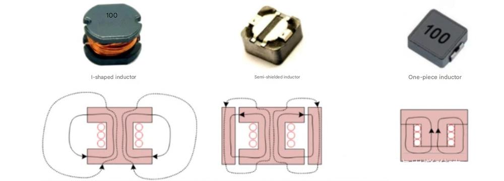
How to choose in work, first of all, you need to understand the structure of the inductor. The inductors we commonly use include non-shielded I-shaped inductors, semi-shielded inductors, and body-molded inductors. What are their characteristics?

① I-shaped inductors, the magnetic circuit is composed of a magnetic core and air, and its magnetic flux lines are completely exposed to the air without any magnetic shielding
② Semi-shielded inductors, as can be seen from its skeleton structure, are based on I-shaped inductors, and magnetic shielding materials are added to the periphery of the inductor. Because the magnetic resistance of the magnetic shielding material is small, the magnetic flux lines are basically locked in the magnetic conductive material, and only a small part of the magnetic field will leak out from the air gap, so it can play a certain shielding role.
③ One-piece molded inductors, when the inductor is produced, the winding and the magnetic conductive material are cast at one time, and there is only a small air gap inside to prevent the inductor from saturating, so this type of inductor basically has no magnetic flux lines overflow.
The effect of copper skin on the inductance of non-shielded I-shaped inductors and shielded inductors was experimentally tested, and it was found that the inductance of the non-shielded I-shaped inductor was reduced under the condition of copper skin, while the shielded inductor had almost no effect.
What effect does copper plating on the bottom of the inductor have on the power supply?
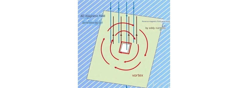
Before thinking about this question, you need to understand the eddy current effect. When the magnetic flux lines are from N to S level and there is an alternating magnetic field passing through the surface of the conductor, the law of electromagnetic induction shows that an induced current is formed on the surface of the conductor, and the direction of the magnetic field generated by the induced current will always weaken the size of the original magnetic field.

Take a boost DCDC circuit + current loop as an example to talk about the effect of copper plating on the bottom of the inductor on the power supply design.
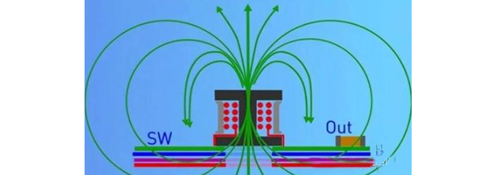
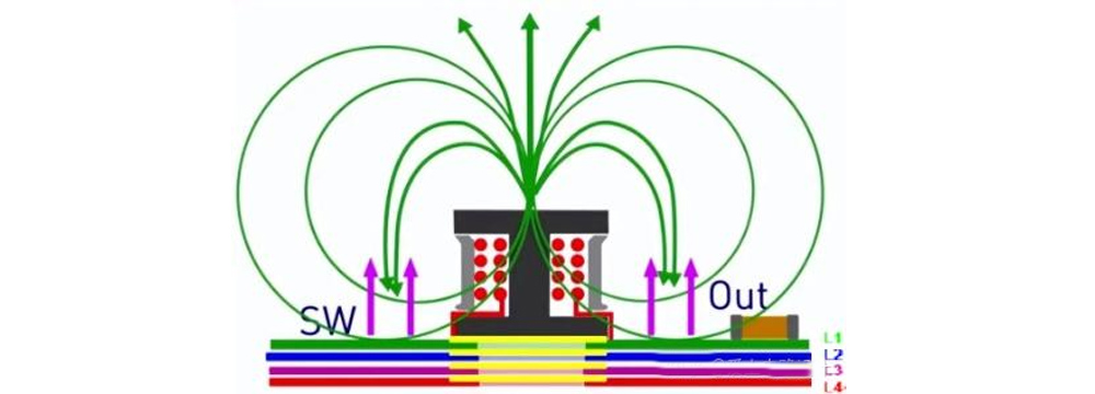
When the boost works normally, the load current flows through the inductor to form a loop. Due to the presence of the switch tube, the current changes dynamically, which can form the magnetic flux lines of the inductor. On the surface of the conductor, some of the magnetic flux lines form a closed magnetic loop, and some of the magnetic circuits will form leakage magnetic flux overflowing into the air. If there is no copper plating on the bottom of the inductor, the magnetic flux lines overflowing from the inductor will exist in the entire power supply system, leaving the system without a relatively quiet space, resulting in a decrease in EMI performance.

If the bottom of the inductor is covered with complete copper, an eddy current effect will be generated on the plane at the bottom of the inductor. The eddy current will offset the magnetic field generated by part of the leakage inductance, weakening the original leakage magnetic induction line. The eddy current generated by the copper coating at the bottom of the inductor is like an electromagnetic shield, blocking the magnetic induction line from propagating downward. Therefore, the high-frequency magnetic field generated by the inductor can be shielded on one side of the conductor, which greatly reduces the impact of the high-frequency magnetic field on other components in the space.

From two perspectives, from the perspective of EMI, it is recommended to coat copper; from the perspective of inductance, the shielded inductor has no effect on the inductance, so it is also recommended to coat copper, and only the bottom of the I-shaped inductor has a slight effect on the inductance, so it depends on the situation in the actual project.
In the actual PCB layout, the filter at the switch is placed on the PCB plane opposite to the inductor, which is more conducive to avoiding high-frequency interference filtering components and preventing high-frequency interference from being transmitted through the line.
Not only DC-DC isolated power supplies, but generally all isolated switch power supplies need to add this capacitor. Transformers are used in isolated power supplies. There is a tiny parasitic capacitor between the primary and secondary sides of the transformer. The common-mode interference generated by the switch circuit in the primary circuit of the switching power supply during operation will be transmitted to the secondary circuit of the secondary side through this parasitic capacitor. There is also a parasitic capacitor between the secondary circuit and the earth. Then the common-mode interference will flow back to the earth through this parasitic capacitor, thus forming a conducted interference to the external power supply network, which will be measured by the instrument during EMI measurement.
If a capacitor is added between the primary and secondary sides of the transformer, a nearby return path is provided for the interference, which can reduce the energy of the common-mode interference flowing from the secondary circuit to the earth, thus reducing the external interference.
Share our interesting knowledge and stories on social media


