Introduction to high-frequency inverters
High-frequency inverters use high-frequency DC/AC conversion technology to convert low-voltage DC power into high-frequency low-voltage AC power. After being stepped up by a high-frequency transformer, the high-frequency inverter is rectified into high-voltage DC power, which is usually above 300V, and finally rectified into 220V AC power for the load through an industrial frequency inverter circuit. Advantages and disadvantages of high-frequency inverters: High-frequency inverters use small-volume and light-weight high-frequency magnetic core materials, which greatly improves the power density of the circuit, making the no-load loss of the inverter power supply very small and improving the inverter efficiency. Usually, the peak conversion efficiency of high-frequency inverters reaches more than 90%. However, it also has significant disadvantages. High-frequency inverters cannot be connected to fully loaded inductive loads and have poor overload capacity.
Classification of high-frequency inverters
(1) Square wave inverters
The AC voltage waveform output by square wave inverters is a square wave. The inverter circuits used by this type of inverter are not exactly the same, but the common feature is that the circuit is relatively simple and the number of power switch tubes used is small. The design power is generally between hundreds of watts and kilowatts. The advantages of square wave inverters are: simple circuit, low price, and easy maintenance. The disadvantage is that since the square wave voltage contains a large number of high-order harmonics, additional losses will be generated in load appliances with iron core inductors or transformers, which will interfere with radios and certain communication equipment. In addition, this type of inverter has disadvantages such as insufficient voltage regulation range, imperfect protection function, and relatively large noise.
(2) Step wave inverter
The AC voltage waveform output by this type of inverter is a step wave. There are also many different circuits for the inverter to achieve step wave output, and the number of steps in the output waveform varies greatly. The advantage of the step wave inverter is that the output waveform is significantly improved compared to the square wave, the high-order harmonic content is reduced, and when the number of steps reaches more than 17, the output waveform can achieve a quasi-sine wave. When a transformer-free output is used, the overall efficiency is very high. The disadvantage is that the step wave superposition circuit uses more power switch tubes, and some of the circuit forms also require multiple groups of DC power input. This brings troubles to the grouping and wiring of the solar cell array and the balanced charging of the battery. In addition, the step wave voltage still has some high-frequency interference to radios and some communication equipment.
Scope of use of high-frequency inverter
Currently, most commercially available high-frequency inverters can provide waveforms. This type of quasi-sine wave inverter can be used in laptops, TVs, audio equipment, cameras, digital cameras, car refrigerators, printers, various chargers, handheld computers, game consoles, DVD players, and mobile DVDs.
Principle of the circuit diagram of the rear stage of the high-frequency inverter
The basic function of the rear stage circuit is to invert the high-voltage DC boosted by the front stage into AC. From the structural point of view, the full-bridge structure is the most used.
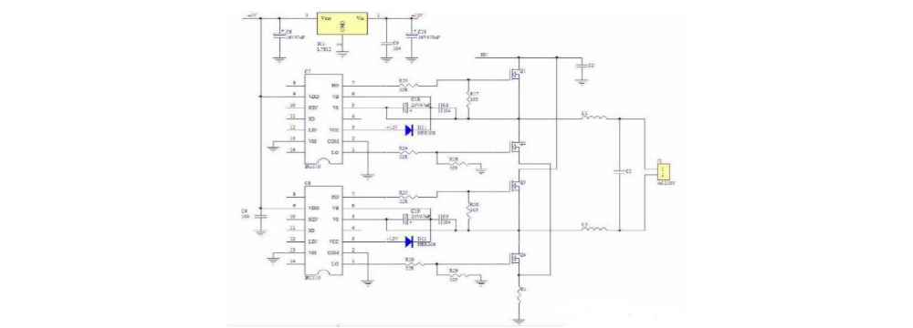
The following is an example of the rear stage circuit of the single-phase sine wave inverter. Some circuits are shown in the figure below:

1. The impact of Miller capacitors on the safety of high-voltage MOS tubes and their solutions
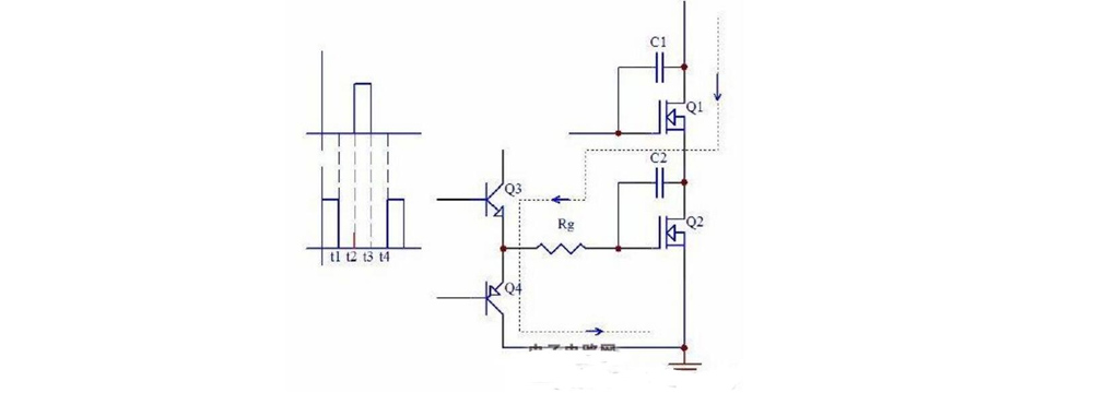
I remember that many netizens mentioned that IR2110 is very unstable in driving full-bridge MOS, and often explodes inexplicably. It is often fine during low-voltage tests, but it explodes as soon as the bus voltage is increased. This is indeed a very headache problem. Let's first analyze the effect of the MOS tube GD junction capacitance, also known as Miller capacitance, on the upper and lower switches of the half-bridge. The circuit for analysis is as follows:

In the figure, C1 and C2 are the GD junction capacitances of Q1 and Q2 respectively, and the upper and lower waveforms on the left are the gate drive waveforms of Q1 and Q2 respectively. Let's start the analysis from the t1-t2 dead zone. It can be seen from the figure that this period is the dead zone time, that is, during this period, both tubes are not turned on, and the voltage at the midpoint of the half-bridge is half of the bus voltage, that is, the charging of C1 and C2 is also half of the bus voltage. When the drive signal runs to t2, the gate of Q1 becomes high level, Q1 starts to turn on, the potential at the midpoint of the half-bridge rises sharply, C2 is charged by the bus voltage, and the charging current passes through the drive resistor Rg and the drive circuit discharge tube Q4. This charging current will generate a burr voltage on the drive resistor Rg and the drive circuit discharge tube Q4. Please see the red vertical line at t2 in the figure. If the amplitude of this glitch voltage exceeds the Qth of Q2's turn-on voltage, the upper and lower tubes of the half-bridge will be connected. Sometimes, a slight connection between the upper and lower tubes will not necessarily cause the tube to explode, but it will cause the power tube to heat up, and obvious interference glitches will be seen on the bus with an oscilloscope. The tube will only explode when the connection is more serious. Another feature is that the higher the bus voltage, the higher the glitch voltage, and the more likely it will cause the tube to explode. Now that everyone knows the principle of the generation of this glitch voltage, I think it is easy to solve this problem. There are three main solutions:
1) Use a gate active clamp circuit. You can directly use a low-resistance MOS tube to pull down the gate of the MOS tube to make it turn on in the dead zone;
2) Use RC or RCD absorption circuit;
3) Add negative voltage to the gate to turn off. This is the best way. It can shift the glitch voltage to below the source level through level shifting, but the circuit is more complicated.
2. Issues that need to be noted in the application of IR2110
IR2110 is a half-bridge driver launched by IR Company in the early stage. It has the advantages of low power consumption, simple circuit, fast switching speed, etc. It is widely used in the full-bridge drive of the inverter. For the application of IR2110 in DIP16 package in sine wave inverter, the following points should be paid attention to:
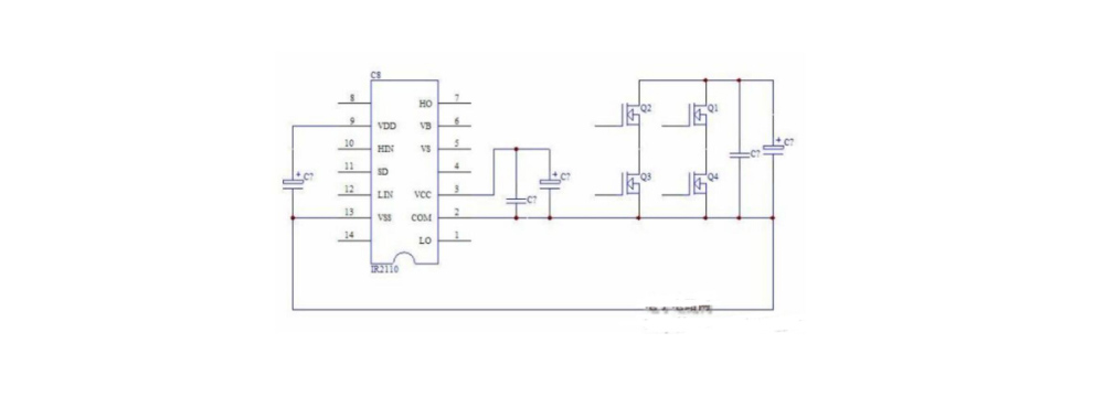
1) The logic ground of pin 13 and the drive ground of pin 2 should be separated during wiring. The logic ground is generally connected to the negative end of the 5V filter capacitor, and then to the negative end of the high-voltage filter capacitor. The drive ground is generally connected to the negative end of the filter capacitor of the 12-15V drive power supply, and then to the source of the farther MOS of the two low-end high-voltage MOS tubes. As shown below:

2) In the sine wave inverter, because the frequency of the carrier is high and the bus voltage is also high, the bootstrap diode should use a high-frequency and high-voltage diode. Because the carrier duty cycle is close to 100%, the capacity of the bootstrap capacitor should be calculated according to the fundamental wave, generally 47-100uF is required, and a small high-frequency capacitor is best connected in parallel.
3. Calculation of LC filter parameters for sine wave inverters
It is indeed a tedious task to accurately calculate the parameters of the LC filter for sine wave inverters. Here I introduce a set of approximate and simple calculation methods, which have also been proven to be feasible in actual tests. My idea is that the filter inductance of SPWM is similar to the output filter inductance of the forward-type switching power supply, except that the pulse width of SPWM is variable, and the filtered voltage is a sine wave instead of a DC voltage. If we calculate according to the point where the inductor ripple current is the largest within half a sine cycle, I think it is feasible. The following is an example of calculating the parameters of the LC filter using a 1000W 220V sine wave inverter. The following physical quantities are introduced first:
Udc: Input voltage of the inverter H bridge, the range of variation is about 320V-420V;
Uo: Output voltage, 0-311V, effective value is 220V;
D: Duty cycle of the SPWM carrier, which changes continuously according to the sine law;
fsw: Switching frequency of SPWM, taking 20kHz as an example;
Io: Output current, the peak current of the inductor is about 1.4Io;
Ton: The conduction time of the switch tube, which actually changes continuously according to the sine law;
L: The inductance required by the LC filter;
R: Load resistance of the inverter.
So we have:
L=(Udc-Uo)Ton/(1.4Io)(1)
D=Uo/Udc(2)
Ton=D/fsw=Uo/(Udc*fsw)(3)
Io=Uo/R(4)
Combining (1), (3), (4), we have:
L=(Udc-Uo)*Uo/(1.4Io*Udc*fsw)=R(1-Uo/Udc)/(1.4fsw)
For example, for an inverter with an output power of 1000W, assuming that the minimum load is 15% of the full load, then R =220*220/(1000*15%)=323Ω
From L=R(1-Uo/Udc)/(1.4fsw), it can be seen that L=0 at the moment of Uo=Udc, and no inductance is needed; the smaller the Uo, the larger the L required. We can compromise and take L=323*(1-0.5)/(1.4*20000)=5.8mH when Uo=0.5Udc. This value is calculated based on the continuous calculation of the inductor current when the output is 15%Io, so it is relatively large and can be corrected according to the minimum load of the inverter. For example, if the minimum load is half load 500W, L only needs 1.7mH.
After determining the filter inductance, we can determine the filter capacitor C. The determination of the filter capacitor C is relatively easy. Basically, it is calculated based on the filter cutoff frequency of 5-10 times the fundamental wave. The calculation formula is

Share our interesting knowledge and stories on social media


