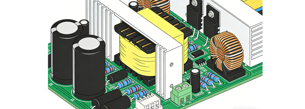
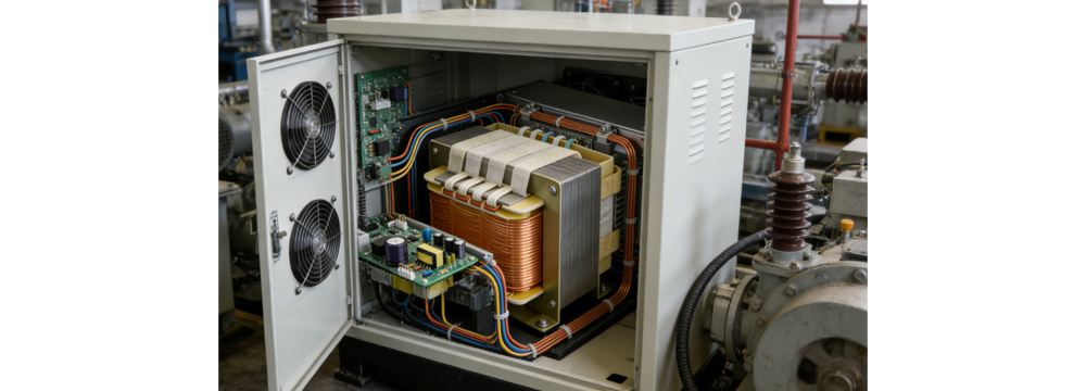
In the field of high-voltage power supply design, noise issues have always been a key bottleneck restricting the improvement of product performance. When the operating voltage of a power supply exceeds 1000V, even minor layout defects may cause problems such as excessive electromagnetic interference (EMI) and signal distortion, which not only affect the normal operation of surrounding equipment but also shorten the service life of the power supply itself. As a core means of controlling noise from the source, PCB layout optimization is far more than just "organizing circuits". Instead, through the refined design of current paths, reference planes, and component placement, it builds a complete "noise suppression system", enabling high-voltage power supplies to achieve low-noise output while operating efficiently.
1. Optimizing Current Loops: Cutting Off the "Physical Path" of Noise Generation
In high-voltage power supplies, large currents generate intense voltage fluctuations during switching processes. If the current loop design is unreasonable, it is easy to form a "noise radiation antenna". Traditional layouts often result in long current paths and numerous corners due to the scattered placement of power components. However, optimized PCB layouts prioritize shortening the length of high-frequency power loops. For example, IGBT modules, rectifier bridges, and filter capacitors are closely arranged, controlling the area of the main power loop within 5 cm². This design can significantly reduce loop inductance and minimize the peak voltage noise caused by di/dt changes. Taking a 1500V photovoltaic inverter as an example, the inductance of the main power loop before optimization reaches 80nH, and the voltage spike generated during the switching process exceeds 300V. By directly mounting the filter capacitor near the pins of the IGBT module, the loop inductance is reduced to below 20nH, and the amplitude of the peak noise is reduced by more than 60%.
At the same time, for different types of current loops in high-voltage power supplies, layout optimization also adopts an "isolated design". For instance, control signal loops and power current loops are arranged separately to avoid crossing and overlapping, preventing strong electromagnetic interference generated by power loops from coupling into control loops. In the design of a certain 2000V industrial power supply, initially, the control chip was placed too close to the power resistor, leading to interference in the PWM control signal and output voltage ripple exceeding 5%. After adjusting the layout, the control circuit and power circuit were placed in separate areas along the edge of the PCB, with a 3mm-wide "isolation zone" reserved between them. Finally, the output ripple was reduced to below 1%, fully meeting the stability requirements of industrial equipment for power supplies.
2. Optimizing Reference Planes: Building a "Protective Net" for Noise Shielding
Reference planes (especially ground planes) play the role of "noise absorbers" in high-voltage power supply PCBs. Unreasonable reference plane design will increase ground impedance, making it impossible for noise to be effectively discharged. During layout optimization, a "complete ground plane" design is prioritized, avoiding random 开窗 (windowing) or segmentation on the ground plane to ensure a low-impedance return path for current. For high-voltage power supplies that require multi-power supply partitioning, such as equipment containing both a 3.3V control power supply and a 1200V main power supply, a "star grounding" method is adopted. The grounding terminals of different voltage levels are centrally connected to the same grounding point to prevent noise from different loops from crosstalking with each other through the ground plane.

In addition, the "interlayer matching" of reference planes is also a key optimization focus. In multi-layer PCB design, high-voltage power layers are arranged adjacent to ground planes, and the parasitic capacitance between them is used to achieve noise filtering. Taking a 10-layer PCB high-voltage power supply as an example, during layout, the 1200V power layer (PWR1) is placed adjacent to the ground plane (GND1), and the 3.3V control power layer (PWR2) is adjacent to another ground plane (GND2). This "power layer - ground plane - control layer - ground plane" stacking method can prevent high-voltage power noise from spreading to the control circuit through the shielding effect of the ground plane. Test data shows that the radiated emission (RE) of the power supply with this layout is reduced by 15-20dBμV/m in the 30MHz-1GHz frequency band compared with the traditional layout, easily passing EMC certification tests.
3. Optimizing Component Placement: Reducing Noise "Excitation Sources" from the Source
There are various types of components in high-voltage power supplies, and the noise characteristics of different components vary greatly. Layout optimization conducts "classified placement" based on component functions and noise levels to reduce noise generation from the source. For switching components that are prone to generating noise (such as SiC MOSFETs), they are centrally placed on the edge of the PCB and kept away from noise-sensitive components such as sampling resistors and voltage sensors. The distance between them is at least 10mm to avoid high-frequency noise generated during the switching process from directly coupling into the sampling loop. In the design of a certain 1200V SiC power supply, initially, the SiC MOSFET and the current sampling resistor were placed adjacent to each other, resulting in a large amount of high-frequency noise mixed into the sampling signal, and the current detection error exceeded 8%. After adjusting the layout, the distance between them was increased to 15mm, and a grounded copper sheet was set in the middle for isolation. The sampling error was reduced to within 2%, ensuring the accuracy of current control.

At the same time, the "orientation arrangement" of components also affects the noise level. For components such as high-voltage capacitors and inductors, during layout, their pin directions are aligned with the current flow direction to reduce the number of lead bends and lower parasitic inductance and capacitance. For example, when placing high-voltage electrolytic capacitors, the positive pin is directed directly to the input end of the power component, and the negative pin is directly connected to the ground plane, avoiding current path distortion caused by pin crossing. Although this detailed optimization seems minor, it can significantly reduce noise in high-frequency switching scenarios. Experimental data shows that the conducted emission (CE) of the power supply with optimized component orientation is reduced by 10dBμV in the 150kHz-30MHz frequency band compared with disorderly arrangement, further improving the electromagnetic compatibility of the power supply.
4. Optimizing Wiring Strategies: Refining the "Final Link" of Noise Control
Wiring is the final link in PCB layout optimization and a "key detail" in noise control. In high-voltage power supply wiring, the principle of "wide wire diameter and short path" is adopted. For power wires carrying large currents, the wire diameter is determined based on the current size (usually 2A per square millimeter of copper foil), avoiding excessive current density caused by too thin wire diameters and reducing noise caused by Joule heat. At the same time, power wires avoid right-angle and acute-angle bends as much as possible, using 45° angles or arc transitions to reduce parasitic inductance of the wiring. A right-angle bend can increase the equivalent inductance of the wiring by 10%-15%, while an arc transition can control the inductance increase within 5%, effectively reducing the radiation of high-frequency noise.
For differential signal wiring (such as differential pairs for voltage sampling), a "equal length and equal spacing" parallel wiring method is adopted to ensure that the parasitic parameters of the two wires are consistent and reduce the impact of common-mode noise. In the voltage sampling loop of a certain high-voltage power supply, initially, the length difference of the differential wiring exceeded 5mm, leading to common-mode noise interfering with the sampling signal and reducing the output voltage regulation accuracy. By adjusting the wiring to control the length difference of the two wires within 1mm and maintaining a spacing of 2mm, common-mode noise was significantly suppressed, and the voltage regulation accuracy was improved from ±2% to ±0.5%. In addition, during wiring, an "array of grounded vias" is set under key wires (such as PWM control signals). Through the vias, the wires are closely connected to the ground plane to form a "microstrip line" structure, further enhancing the shielding effect against noise.
In conclusion, PCB layout optimization plays the role of a "systematic solution" in noise reduction for high-voltage power supplies. It is not a single technical means but comprehensively controls noise from multiple links such as noise generation, propagation, and coupling through the collaborative optimization of current loops, reference planes, component placement, and wiring strategies. With the development trend of high-voltage power supplies towards high frequency and miniaturization, the importance of PCB layout optimization will become increasingly prominent. Only by deeply combining layout design with power supply topology and component characteristics can we truly achieve the "high efficiency, low noise, and stability" performance goals of high-voltage power supplies and provide more reliable power supply solutions for new energy, industrial control, aerospace, and other fields.
Share our interesting knowledge and stories on social media


